OrbitalHub

Where curiosity reaches escape velocity.

Domain is for sale. $50,000,000.00 USD. Direct any inquiries to contact@orbitalhub.com.

Archive for the Computing category


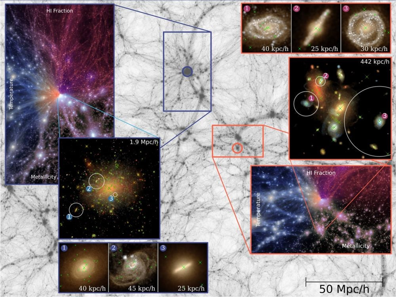
Visualization of the ASTRID simulation at z=0. The underlying image is dark matter density, with insets showing a most-massive-halo zoom, gas maps of temperature and metallicity, and a mock Hubble observation. Credit: ASTRID / Zhou et al. 2026, ApJ.


On a Texas supercomputer this summer, a 370 Mpc/h cube of dark matter, gas, and stars finished a 13.5-billion-year journey. The run began at redshift z=99, when the cosmos was a thin hydrogen-helium plasma and the first stars had not yet ignited. It ended at z=0, with galaxy clusters, supermassive black holes, and the cosmic web we see today. The team calls the simulation ASTRID, and the final z=0 dataset was published in The Astrophysical Journal in February 2026, with a public release coordinated through the Texas Advanced Computing Center on August 27, 2026 (Zhou et al., ApJ, 2026).

The headline numbers are easy to recite. ASTRID evolves 2 × 5500³ ≈ 0.33 trillion particles in a 370 Mpc/h box. Each simulation snapshot totals 30 TB. The archived state across the run is measured in petabytes. Less obvious is what those numbers actually buy the cosmologist at the other end of the keyboard: a single dataset that connects the universe’s first black hole seeds to the billion-solar-mass monsters sitting in galactic centers today.

JWST keeps pulling ancient quasars and “Little Red Dots” out of the early universe that do not fit the old growth timelines. The first JWST surveys suggested that 10⁹ M☉ black holes already existed at z > 8, hard to reconcile with seed models from a decade ago (Naidu et al., 2024, and follow-ups). To make sense of those objects, theorists need a model universe that can track baryons, gas cooling, star formation, and black hole accretion from cosmic dawn to the local universe, all at high enough resolution to capture the small dark-matter halos where the first quasars lit up.

Cosmological simulations do that, but they are expensive. Each box has to be large enough to contain rare massive clusters, dense enough to track small galaxy halos, and long enough to evolve them across 13.5 Gyr. Few projects manage all three at once. ASTRID does.

Yihao Zhou, a PhD student at Carnegie Mellon University’s McWilliams Center for Cosmology and Astrophysics, led the run. His advisor, Tiziana Di Matteo, is the principal investigator and the center’s director. The team used the NSF-funded Frontera system at the Texas Advanced Computing Center (TACC) under a 2024 Leadership Resource Allocation (TACC press, August 27 2026).

The run sits in a crowded field. MillenniumTNG’s flagship covers 740 Mpc per side, roughly eight times the volume. IllustrisTNG-300 uses a similar box size with less dark-matter resolution. Eagle is smaller but uses higher resolution per particle. MassiveBlack-II covers 533 Mpc with far fewer particles and no full hydrodynamic run to z=0. ASTRID’s pitch is that no other published run combines this particle count, this box size, and a continuous evolution to z=0 with a complete black hole sub-population (Zhou et al., 2026).

That black hole population is the part astronomers care most about. ASTRID carries massive black holes (MBHs) spanning 4 × 10⁴ to 2 × 10¹¹ M☉, the range from putative seeds to the heaviest known monsters. Earlier ASTRID snapshots have already shown up in papers on Little Red Dot analogs (Hassan et al., Open Journal of Astrophysics, 2025) and on black hole merger rates that match LISA predictions. Mock JWST and Euclid light-cones built from the simulation give observers a template to compare against real survey catalogs, which is how the team plans to constrain the seed-black-hole mass in the next round of analyses.

ASTRID is a smoothed-particle hydrodynamics (SPH) simulation, which means the gas and dark matter are discretized into Lagrangian particles that move with the flow. The code solves the Euler fluid equations coupled to a particle-mesh gravity solver. Long-range forces use a coarse mesh; short-range forces use a hierarchical Barnes-Hut octree that drops subtrees whose multipole moments fall below an opening-angle tolerance θ.

The sub-grid physics is where most of the engineering sits. Gas above a density threshold around 0.1 cm⁻³ is converted into stars using a Kennicutt-Schmidt-style surface-density law, Σ_SFR ∝ Σ_gas^n with n ≈ 1.4. Black holes are seeded in dark-matter halos above ~5 × 10¹⁰ h⁻¹ M☉ and accrete via a Bondi-Hoyle-Lyttleton prescription capped at the Eddington rate:

Mdot_BH = min( Mdot_Bondi, Mdot_Edd ) = min( 4π G² M_BH² ρ / (c_s² + v²), L_Edd / (ε c²) )

Feedback comes in two flavors. Thermal quasar-mode kicks in at high accretion (≳1% of Eddington), kinetic jet-mode at low accretion. That thermal-versus-kinetic split is what produces the bimodal color sequence between star-forming blue galaxies and quiescent red ones.

The dynamical-friction submodel is the piece most relevant to LISA. When two galaxies merge, their central black holes are flung into a wide orbit. Chandrasekhar’s formula determines how fast each black hole sinks into the merger remnant:

df/dt = -4π G² M_BH² ρ(r) ln(Λ) f(v) / v²

The Coulomb logarithm Λ runs ~3-5 for galaxy mergers. Without this term, ASTRID would smear the merger-rate signal that LISA wants to hear.

LISA’s sensitivity band runs from ~10⁻⁴ Hz to ~10⁻¹ Hz, the regime populated by MBH mergers of 10⁴ to 10⁷ M☉ across cosmic time. Di Matteo’s earlier work (Ni et al. 2022) projected ~30 MBH mergers per year detectable by LISA out to z ≈ 10. The full z=0 ASTRID data set should sharpen that number, and provide a sky-position catalog that future gravitational-wave observers can cross-match against electromagnetic transients (Zhou et al., 2026).

On the engineering side, Frontera is the largest NSF open-science cluster in the United States. Built around Intel Cascade Lake Xeon nodes with ~60 PB of Lustre storage, it absorbed ASTRID’s 30 TB snapshots without complaint (TACC user guide, August 4 2026). The team’s next target is TACC’s Horizon system, the NSF Leadership-Class Computing Facility machine deploying in two phases (GPU first, then CPU) later in 2026. The ASTRID code is currently CPU-only; Zhou and colleagues are rewriting the gravitational and black-hole feedback kernels to run on NVIDIA GPUs.

For years, astrophysicists have asked how supermassive black holes got so big, so fast. ASTRID does not answer that on its own, but it gives the community a 0.33-trillion-particle laboratory to test the answers against.

The next year or two will bring a GPU port to Horizon, plus companion runs at higher resolution or with varied cosmological parameters. By the time LISA Pathfinder’s successor launches around 2035, theorists will want catalogs like ASTRID’s to interpret the gravitational-wave sky.

What comes out of a simulation like this is rarely a single discovery. It is a reference. A way for theorists to ask whether their model matches what we should see, with enough resolution to be honest about the mismatch. ASTRID is now that reference for the next decade of SMBH and gravitational-wave cosmology.
 

September 21, 2026

Rapidus, IBM, and Japan’s 2nm gamble

Posted by


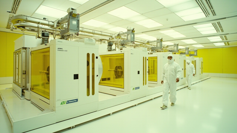
A row of EUV lithography scanners inside a modern semiconductor cleanroom, similar to the equipment installed at Rapidus's IIM-1 pilot fab in Chitose, Hokkaido.


For the past year, the headlines about leading-edge chips have read like a closed case. TSMC pulled the first 2 nm wafers off its Hsinchu line in late 2025, with Apple taking the first slice. Samsung’s competing gate-all-around (GAA) node followed shortly after. Intel’s 18A staggered through yield issues. The story was supposed to be a foundry duopoly asserting itself once again.

Then there is a small company in Chitose, Hokkaido, with a cleanroom the size of an aircraft hangar and a different idea about how a fab should run. Rapidus is trying to do something the rest of the industry has decided is impossible: build leading-edge logic chips one wafer at a time, ship a customer’s design back in fifty days, and enter mass production in 2027, about two years behind the leaders. The bet is not that Japan can outspend Taiwan. It is that some chip buyers no longer want a foundry that treats them like a queue number.

Three things are happening at once. Demand for AI training and inference silicon is growing roughly 30 percent a year. Geopolitics is making the concentration of leading-edge fabs in one corner of the Pacific a strategic liability. And the cost of a new fab has crossed the line where only a sovereign wealth fund, the U.S. CHIPS Act, or a national budget can write the check. TSMC is on track to push 2 nm capacity past 100,000 wafers a month by the end of 2026 and is already sampling A16 (1.6 nm) with backside power delivery to its largest customers.

That concentration is what Rapidus was created to dilute. The Japanese government has put in roughly 1.4 trillion yen directly. Private investors added 920 billion yen in a February 2026 round, taking cumulative support past 2.35 trillion yen. Sony, Toyota, Kioxia, Denso, NEC, SoftBank, and Canon now sit on the shareholder list. The state is the largest single holder.

What they bought is a thesis: that the foundry business can be unbundled. Volume production belongs to TSMC and Samsung. Fast-turn prototyping and small-batch manufacturing for AI startups and Japanese industrial customers can be a separate business. Tenstorrent, the AI chip company led by Jim Keller, signed on as an early customer. Canon became the first major Japanese anchor in March 2026 with a 40 billion yen joint program for image-processing silicon.

Rapidus did not start as a chip company. It started in 2022 as a question inside Japan’s Ministry of Economy, Trade and Industry: who would build the country’s processors if access to TSMC at 5 nm and below were cut off? In roughly eighteen months, the answer became a state-backed foundry that would license IBM’s most advanced transistor design and build a cleanroom around it.

The IBM connection is the keystone. In May 2021, IBM demonstrated a 2 nm test chip on a GAA nanosheet architecture at its Albany NanoTech Complex in New York, a research fab jointly funded by IBM, the State University of New York, and a rotating set of equipment vendors. Albany is a lab, not a production line. IBM has not owned a fab since selling its chip business to GlobalFoundries in 2015. It needed a partner willing to take its research and run it for real.

Rapidus signed on in December 2022 and sent 150 engineers to Albany for two years; half have now rotated back. The cleanroom, IIM-1 (Innovative Integration for Manufacturing), broke ground in September 2023. The first ASML NXE:3800E extreme ultraviolet (EUV) scanner arrived in December 2024 and printed its first wafer in April 2025. By July 18, 2025, Rapidus had working 2 nm GAA transistors on a prototype wafer, with electrical characteristics the company said met its targets (Rapidus press release, July 2025).

The harder work has come since. CTO Kazunari Ishimaru acknowledged in a March 2026 interview that the July 2025 milestone had been announced “ahead of full readiness,” with significant work done between September and November 2025 to bring transistor performance in line. A Process Design Kit went out to customers in Q1 2026. Customer test chips are scheduled to start running in late 2026, with mass production targeted for the second half of 2027.

The pricing target is roughly 3 to 3.5 million yen per wafer, a 50 percent premium over TSMC’s mature nodes but reportedly competitive with N2. Capacity is 6,000 wafer starts per month initially, ramping to 25,000 in the first year. To put that in scale, TSMC’s 2 nm output alone is expected to exceed 100,000 wafers a month by mid-2026. Rapidus is not trying to match that volume. It is trying to make the customer interaction different.

The reason Rapidus is in the conversation at all is the transistor. For twenty years the industry rode a structure called FinFET: a vertical fin of silicon with the gate wrapped around three sides. FinFETs scaled cleanly to about 5 nm. Below that, leakage through the bottom of the fin starts to dominate, and the supply voltage V_DD cannot drop further without losing switching speed.

A gate-all-around nanosheet transistor solves this by replacing the fin with a stack of thin horizontal silicon sheets, each fully surrounded on all four sides by the gate stack. The electrostatic coupling between gate and channel is described by a term called the subthreshold swing, and the relevant limit is

S = (kT / q) * ln(10) * (1 + C_dep / C_ox)

where kT / q is the thermal voltage (about 26 mV at room temperature), C_dep is the depletion capacitance in the channel, and C_ox is the gate oxide capacitance. As C_ox grows relative to C_dep, S falls toward 60 mV per decade, the theoretical minimum, and off-state leakage drops with it. Wrapping the gate on all four sides drives C_ox up, which is why GAA is the only way to keep scaling below 3 nm.

The engineering cost is enormous. GAA nanosheets require multiple epitaxial growth steps, selective layer reductions to set the threshold voltage, and extreme ultraviolet lithography at a 13.5 nm wavelength. Each NXE:3800E EUV scanner costs roughly 200 million dollars and runs at about 195 wafers per hour. Rapidus has installed more than 200 such tools in IIM-1 in less than a year.

Single-wafer processing, moving each wafer through every step individually rather than batching in lots of 25, is the other bet. Batch processing is faster per step but extends the cycle time. A typical TSMC N3 wafer takes about 120 days from order to delivery; Rapidus is targeting 50. Achieving that means tighter scheduling, more material-handling automation, and a manufacturing execution system that can coordinate several hundred tool types in real time.

Rapidus will probably not threaten TSMC’s volume business. Apple alone will consume more 2 nm wafers in 2026 than Rapidus plans to ship in its first year of mass production. The geopolitical and ecosystem advantages TSMC has built are not moveable in a single fab cycle.

What Rapidus may do is create a third option for chip designers who have spent a decade with two. Tenstorrent’s bet is that fast tape-out and design-manufacturing co-optimization can compress the time between a new AI model and a chip that runs it. Canon’s bet is that having a domestic 2 nm source for image processing matters more than having the cheapest one. The state’s bet is that 2.35 trillion yen is worth the option of not being locked out of the leading edge by 2030.

Whether any of these bets pay off will be visible in the defect density charts of late 2027. Until then, the most interesting question in semiconductors is not who is winning the 2 nm race. It is whether there is room for someone who is not in it at all.