


For the past year, the headlines about leading-edge chips have read like a closed case. TSMC pulled the first 2 nm wafers off its Hsinchu line in late 2025, with Apple taking the first slice. Samsung’s competing gate-all-around (GAA) node followed shortly after. Intel’s 18A staggered through yield issues. The story was supposed to be a foundry duopoly asserting itself once again.
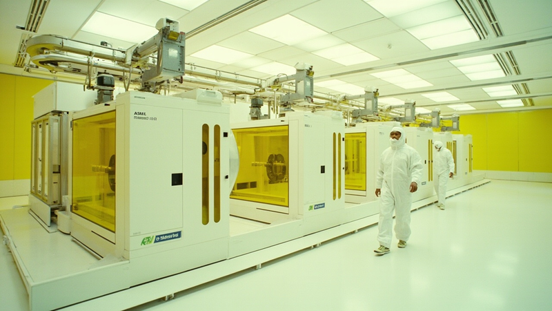
Then there is a small company in Chitose, Hokkaido, with a cleanroom the size of an aircraft hangar and a different idea about how a fab should run. Rapidus is trying to do something the rest of the industry has decided is impossible: build leading-edge logic chips one wafer at a time, ship a customer’s design back in fifty days, and enter mass production in 2027, about two years behind the leaders. The bet is not that Japan can outspend Taiwan. It is that some chip buyers no longer want a foundry that treats them like a queue number.
Three things are happening at once. Demand for AI training and inference silicon is growing roughly 30 percent a year. Geopolitics is making the concentration of leading-edge fabs in one corner of the Pacific a strategic liability. And the cost of a new fab has crossed the line where only a sovereign wealth fund, the U.S. CHIPS Act, or a national budget can write the check. TSMC is on track to push 2 nm capacity past 100,000 wafers a month by the end of 2026 and is already sampling A16 (1.6 nm) with backside power delivery to its largest customers.
That concentration is what Rapidus was created to dilute. The Japanese government has put in roughly 1.4 trillion yen directly. Private investors added 920 billion yen in a February 2026 round, taking cumulative support past 2.35 trillion yen. Sony, Toyota, Kioxia, Denso, NEC, SoftBank, and Canon now sit on the shareholder list. The state is the largest single holder.
What they bought is a thesis: that the foundry business can be unbundled. Volume production belongs to TSMC and Samsung. Fast-turn prototyping and small-batch manufacturing for AI startups and Japanese industrial customers can be a separate business. Tenstorrent, the AI chip company led by Jim Keller, signed on as an early customer. Canon became the first major Japanese anchor in March 2026 with a 40 billion yen joint program for image-processing silicon.
Rapidus did not start as a chip company. It started in 2022 as a question inside Japan’s Ministry of Economy, Trade and Industry: who would build the country’s processors if access to TSMC at 5 nm and below were cut off? In roughly eighteen months, the answer became a state-backed foundry that would license IBM’s most advanced transistor design and build a cleanroom around it.
The IBM connection is the keystone. In May 2021, IBM demonstrated a 2 nm test chip on a GAA nanosheet architecture at its Albany NanoTech Complex in New York, a research fab jointly funded by IBM, the State University of New York, and a rotating set of equipment vendors. Albany is a lab, not a production line. IBM has not owned a fab since selling its chip business to GlobalFoundries in 2015. It needed a partner willing to take its research and run it for real.
Rapidus signed on in December 2022 and sent 150 engineers to Albany for two years; half have now rotated back. The cleanroom, IIM-1 (Innovative Integration for Manufacturing), broke ground in September 2023. The first ASML NXE:3800E extreme ultraviolet (EUV) scanner arrived in December 2024 and printed its first wafer in April 2025. By July 18, 2025, Rapidus had working 2 nm GAA transistors on a prototype wafer, with electrical characteristics the company said met its targets (Rapidus press release, July 2025).
The harder work has come since. CTO Kazunari Ishimaru acknowledged in a March 2026 interview that the July 2025 milestone had been announced “ahead of full readiness,” with significant work done between September and November 2025 to bring transistor performance in line. A Process Design Kit went out to customers in Q1 2026. Customer test chips are scheduled to start running in late 2026, with mass production targeted for the second half of 2027.
The pricing target is roughly 3 to 3.5 million yen per wafer, a 50 percent premium over TSMC’s mature nodes but reportedly competitive with N2. Capacity is 6,000 wafer starts per month initially, ramping to 25,000 in the first year. To put that in scale, TSMC’s 2 nm output alone is expected to exceed 100,000 wafers a month by mid-2026. Rapidus is not trying to match that volume. It is trying to make the customer interaction different.
The reason Rapidus is in the conversation at all is the transistor. For twenty years the industry rode a structure called FinFET: a vertical fin of silicon with the gate wrapped around three sides. FinFETs scaled cleanly to about 5 nm. Below that, leakage through the bottom of the fin starts to dominate, and the supply voltage V_DD cannot drop further without losing switching speed.
A gate-all-around nanosheet transistor solves this by replacing the fin with a stack of thin horizontal silicon sheets, each fully surrounded on all four sides by the gate stack. The electrostatic coupling between gate and channel is described by a term called the subthreshold swing, and the relevant limit is
S = (kT / q) * ln(10) * (1 + C_dep / C_ox)
where kT / q is the thermal voltage (about 26 mV at room temperature), C_dep is the depletion capacitance in the channel, and C_ox is the gate oxide capacitance. As C_ox grows relative to C_dep, S falls toward 60 mV per decade, the theoretical minimum, and off-state leakage drops with it. Wrapping the gate on all four sides drives C_ox up, which is why GAA is the only way to keep scaling below 3 nm.
The engineering cost is enormous. GAA nanosheets require multiple epitaxial growth steps, selective layer reductions to set the threshold voltage, and extreme ultraviolet lithography at a 13.5 nm wavelength. Each NXE:3800E EUV scanner costs roughly 200 million dollars and runs at about 195 wafers per hour. Rapidus has installed more than 200 such tools in IIM-1 in less than a year.
Single-wafer processing, moving each wafer through every step individually rather than batching in lots of 25, is the other bet. Batch processing is faster per step but extends the cycle time. A typical TSMC N3 wafer takes about 120 days from order to delivery; Rapidus is targeting 50. Achieving that means tighter scheduling, more material-handling automation, and a manufacturing execution system that can coordinate several hundred tool types in real time.
Rapidus will probably not threaten TSMC’s volume business. Apple alone will consume more 2 nm wafers in 2026 than Rapidus plans to ship in its first year of mass production. The geopolitical and ecosystem advantages TSMC has built are not moveable in a single fab cycle.
What Rapidus may do is create a third option for chip designers who have spent a decade with two. Tenstorrent’s bet is that fast tape-out and design-manufacturing co-optimization can compress the time between a new AI model and a chip that runs it. Canon’s bet is that having a domestic 2 nm source for image processing matters more than having the cheapest one. The state’s bet is that 2.35 trillion yen is worth the option of not being locked out of the leading edge by 2030.
Whether any of these bets pay off will be visible in the defect density charts of late 2027. Until then, the most interesting question in semiconductors is not who is winning the 2 nm race. It is whether there is room for someone who is not in it at all.
 Subscribe to our RSS feed









There are no comments.
Add A Comment